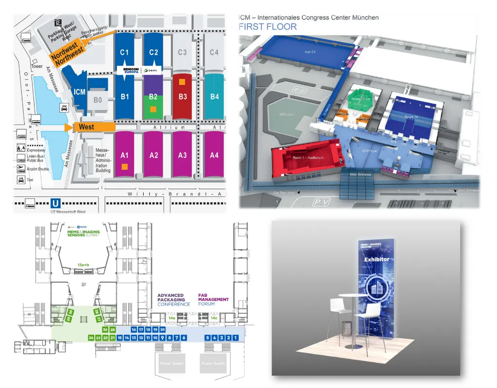
Exhibit at the APC–FMF Expo
ICM International Conference Center (ICM) Foyer, 1st Floor
Wednesday, 11 November 2026
Day 2 of SEMICON Europa
A Prime Sales & Networking Hotspot for 400+ Delegates
Secure your turnkey booth alongside two paid-access conferences—the Advanced Packaging Conference (Room 14a) and Fab Management Forum (Room 14c)—and connect with a 400+ delegate audience in the ICM Foyer.
Date: Wed, Nov 11
Location: ICM, Room 14a
Date: Wed, Nov 11
Location: ICM, Room 14c
Exhibition Overview
2025 Exhibitors

Exhibitor Information
3DiS Technologies
3DiS Technologies offers 3D integration and 3D packaging solutions based on its innovative 3D interconnection technologies. By leveraging the third dimension, the company’s cutting-edge technologies enable miniaturization of electronic systems and passive devices while improving their performance.
Website - 3Dis Technologies
Beneq
Beneq pioneered industrial ALD in 1984. Today, it enables ALD adoption and production with equipment for semiconductor fabrication, R&D, batch processing, and spatial ALD across specialty semiconductors, optics, and functional coatings.
Website - Beneq
Carl Zeiss Microscopy Deutschland GmbH
ZEISS is the only manufacturer worldwide offering light, X-ray, electron, and ion beam microscopy from a single source. With the most comprehensive imaging portfolio in the industry, ZEISS delivers cutting-edge solutions across the entire semiconductor value chain—from wafer fab to packaging and assembly. For mask making and lithography, ZEISS enables zero defect strategies, in-die metrology, and precise overlay control. Its process control and failure analysis tools provide actionable insights to meet the challenges of next-gen semiconductor devices. Globally active ZEISS combines innovation with reliability in optical excellence.
Websites - Semiconductor Microscopy, Semiconductor Manufacturing Technology
CEA-Leti
CEA-Leti (Grenoble, France), a technology research institute at CEA, is a global leader in miniaturization technologies enabling smart, energy-efficient and secure solutions for industry in the fields of transport, health, safety and telecommunications.
Founded in 1967, CEA-Leti pioneers micro-& nanotechnologies, tailoring differentiating applicative solutions for global companies, SMEs and startups. Leti has launched 80 startups.
With a staff of more than 2,000 talents, a portfolio of 3,200 patents, 11,000 sq. meters of cleanroom space and a clear IP policy, Leti has a key role in transferring scientific knowledge and innovation from research to industry, in particular in electronic and integrated systems, from microscale to nanoscale.
Website - CEA-Leti
Comet AG
Comet is a leading global provider of high-end X-ray-based system solutions for non-destructive materials testing in the semiconductor, electronics, automotive, and aerospace industries, as well as for research facilities and scientific institutions. Comet Yxlon inspection solutions help users ensure the quality of their products, optimize their manufacturing processes, and thus increase efficiency and productivity.
The high-precision computed tomography systems for use in the laboratory support research and development and enable detailed structural analysis, metrology applications, and simulation models. The precise microfocus tubes reveal minute details of modern electronic components in the semiconductor and electronics industries.
Website - Home page - Comet
Henkel
Henkel is the premier materials supplier for the electronics assembly and semiconductor packaging industries. Our advanced formulations include a range of products that facilitate electrical interconnect, provide structural integrity, offer critical protection, and transfer heat for reliable performance. We’re proud to create products that improve today’s electronic technologies and enable tomorrow’s advances. Because of the breadth of our materials portfolio, the depth of our application expertise, and the unmatched scope of our global capabilities, the world’s top technology companies - electronics innovators - choose to partner with us.
Website - Semiconductor packaging - Henkel Adhesive Technologies | Henkel Adhesives
ID4US
ID4US delivers Ecrin, a breakthrough biometric system using ultrasonic 3D imaging to create unique digital signatures, redefining standards of security and user experience.
Website - ID4US
LPKF Laser & Electronics SE
Innovative manufacturing technologies for growth markets.
As a high-tech mechanical engineering company, LPKF develops high-precision, scalable manufacturing processes that are used in growth markets such as semiconductors & electronics, life science & medical technology, smart mobility, and research & development. In its 49 years of existence, the company has developed a deep understanding of its customers' needs while relentlessly pursuing innovative solutions to drive technological progress and make a sustainable, positive change in the world.
Website - LIDE® Laser Induced Deep Etching Technology | LPKF
Micron
Micron Technology is a global leader in memory and storage solutions, driving innovation across AI, automotive, mobile and industrial sectors. With a strong presence in Europe, including advanced operations in Germany, Micron offers a dynamic, inclusive workplace where diverse talent thrives. We invest in cutting-edge R&D, sustainability and workforce development to shape the future of technology. As the only U.S.-based memory manufacturer, we empower employees to make a global impact while growing locally. Join us to build smarter, faster and more responsible solutions that enrich lives worldwide.
Website - Micron
Nagase ChemteX America
Nagase ChemteX America, LLC. Is a leading supplier of Negative Tone Photoresists (liquids and films), Electrically Conductive Adhesives, Non-Conductive Adhesives, Dual cure (UV + thermal) Adhesives and Electrically Conductive and Non-Conductive Inks for applications in Semiconductor Packaging, Microcircuit Assembly, MEMS, Microfluidic, Photovoltaic and Printed Electronics markets.
At Nagase ChemteX we have a seasoned staff of polymer chemists, formulators and application engineers to assist you with your most challenging applications.
Website - nagasechemtex.com
Pack4EU / Chips JU / Lab2Fab Pre-Brokerage
Implementation of Pack4EU Recommendations – Pre-Brokerage for upcoming Chips JU Call on R1: Lab2Fab Transfer Accelerator: The Pack4EU Project, answering to Chips JU Work Program 2023 V2 - Call 2023-3-CSA - Topic 2 “Pan-European network for Advanced Packaging made in Europe”, got executed, supported by the Chips JU and its members under grant agreement number 101139933, from 07/2023 – 06/2024. It resulted in 9 recommendations (R1-9). One of them (R1) was an Industrial Transfer Instrument (TRL7+ at Market Readiness) for Advanced Packaging Technology into a) Lab-in-Fab in IDMs and OEMs for captive manufacturing, and b) Open Industrial Piloting Facilities (R4), Packaging Foundries and Services for small/medium volume manufacturing
Website - Pack4EU / Chips JU / Lab2Fab Pre-Brokerage
Promicron GmbH
Promicron is an innovator of automated and semiautomated optical inspection and metrology systems for MEMS Semiconductor industries. Promicron systems efficiently control submicron processes on the WAFER level and DIE level by using AI-supported high-speed micro imaging and spectroscopy in the visible and infrared spectrum.
Inspection
Full Wafer NIR stitching images, high resolution image 8” Wafers in minutes
AOI Infrared inspection of bonded wafers (e.g., bond seal check on the fly)
Metrology
Thickness measurement of films and Si layers
Air gap measurement between bonded wafers
Membrane and cavern inspection
Front-to-back alignment
Overlay and CD measurement
3D microscopy by confocal and interference techniques
Website - promicron.com
SEMI Europe
SEMI is a global industry association that represents the interests of the semiconductor industry's design, manufacturing, and supply chain businesses worldwide, offering various services and products.
One of the most popular products is the industry-recognized benchmark source for monthly semiconductor equipment market data and bi-annual equipment forecasts, such as market data and research reports covering semiconductor equipment, semiconductor materials, semiconductor packaging materials, electronic design market data, as well as wafer fab and packaging materials through SEMI’s Data Collection Programs and with industry partners.
To find out more information, you are welcome to visit us at the SEMI booth as well as review all the different and new reports on the SEMI website: Market Data Reports | SEMI
Website - SEMI Europe
Siemens EDA
Siemens EDA, and represented by EDA Solutions, is a world leader in electronic hardware and software design solutions for the world’s most successful electronic, semiconductor, and systems companies.
The company's MEMS design solution is very popular and sits alongside IC design solutions with outstanding reputations for design, layout, verification and test for image sensors and analog/mixed-signal ICs.
The portfolio includes the following solutions: Analog FastSPICE (AFS), Calibre, Questa, Solido, Symphony, Tanner & Tessent
Website - Siemens EDA
Website - Siemens EDA Solutions
Silex Microsystems
Silex is the World’s largest Pure Play MEMS foundry bringing advanced process technologies and manufacturing capacity to a wide range of high-tech companies Worldwide. MEMS (Micro Electro Mechanical Systems) enable next generation devices and applications in a wide range of market areas such as Medical Devices, Smart Phones, Telecom and other Industrial and Scientific applications. Providing the World’s most impressive technology leaders with state-of-the-art manufacturing services, Silex is a true enabler of the sensory revolution.
Website - Silex Microsystems
Syenta
Syenta introduces Localized Electrochemical Modeling (LEM), a high-speed metallization technology that extends Semi-Additive manufacturing to 1 µm and below. LEM combines localized electrodeposition with micron-resolution stamp-based patterning to enable precise, additive fabrication of redistribution layers (RDLs) and microbumps.
The company was founded in 2022 as a spin-off from The Australian National University, and has its HQ and R&D team in Sydney, Australia.
Website - Syenta
Ushio Inc.
Ushio has garnered a worldwide reputation as a manufacturer of high quality speciality light sources. Covering the entire light spectrum from ultraviolet to infrared, Ushio’s solutions can be found in diverse range of products from cinema projectors and water dispensers to life-saving medical devices, and are used in the production of the latest smartphones and the testing phase of the space industry. Ushio has amassed a wealth of in-house specialist knowledge and localised expertise, irrespective of its global operation, which is of paramount importance when providing lighting solutions that reach far beyond expectations. Simplifying complex processes and fostering partnerships for the long haul is at the heart of what we do. Ushio’s tried and tested approach is to listen to your ideas and to work together with clients to develop world-class bespoke solutions. We are masters in the field of applying light to life.
Website - Ushio Inc.
X-FAB MEMS Foundry GmbH
X-FAB MEMS Foundry is part of the X-FAB Group, the world’s leading analog/mixed-signal foundry, with more than 25 years of experience in integrating a wide range of functionalities such as non-volatile memory, optical sensors, MEMS, and high-voltage transistors. In addition to a broad portfolio of modular CMOS processes with geometries ranging from 0.35 to 0.11 micrometer, X-FAB offers specialized technologies such as SOI, silicon carbide (SiC), and MEMS processes. As a leading MEMS foundry, X-FAB MEMS Foundry provides process technologies for manufacturing micromechanical sensors for detecting pressure, acceleration, rotation, and infrared radiation, among others. It also offers integrated solutions where MEMS sensors are combined with CMOS circuits. In this context, comprehensive solutions for heterogeneous integration (HI) are offered or developed upon customer request for SoC and SoP applications. In Germany, X-FAB currently employs around 1,300 highly qualified staff. Worldwide, approximately 4,500 employees work for the company. Sales offices in key countries across Asia, Europe, and the USA ensure close contact with customers around the globe.
Website - X-FAB
Exhibitor Services
Exhibitor Guide
This guide contains all the essential logistics and details you need as an exhibitor, including booth setup, material shipping, conference registration, and more. Download the guide to ensure you're fully prepared for the event.
Digital Library
Make the most out of your exhibition and take advantage of the graphical material at your disposal. In the digital library, you can find the promotion banners.

Expo Overview
TURNKEY BOOTH RATES
SEMI Member: 3,995 EUR
Non-Member: 4,495 EUR
*All prices in Euro, 19% German VAT excluded
Value Package Rate: Ask us about special package rates that combine the APC–FMF Expo 2026 with the 3D & Systems Summit in June 2027
DELEGATE CONTINGENT
• 1 complimentary delegate pass – Full access to both APC & FMF
• 1 additional delegate pass at 20% off the APC & FMF Flex Pass rate
• Note: Each pass includes a 4-day visitor pass to SEMICON Europa and electronica exhibition halls
BOOTH SPACE & STRUCTURE
• Booth Dimensions: 2m x 2m
• Backlit Fabric Backdrop
• Frame: Aluminum
• Size: 1m (Wide) x 2.5m (High)
• Print: Printing production included (The exhibitor creates design files).
FURNITURE & EQUIPMENT
• Bar Table: 70cm diameter, 1.1m high
• 2 Bar Chairs
• Triple-Socket Power Extension
• Wastebasket